By Power Integrations 149

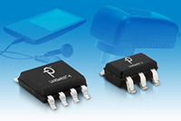
Power Integrations' LinkSwitch-4 family of offline power conversion ICs targets chargers and adapters required to meet stringent new efficiency rules from the US Department of Energy (DoE) and European Code of Conduct (CoC). The new DoE rules, known as DoE-6, require efficiency compliance measurements to be taken at the end of the charger USB cable; LinkSwitch-4 exceeds this requirement while using a low-complexity Schottky diode secondary, even for high-current 1.5 A and 2 A smartphone chargers.
The LinkSwitch-4 family features an advanced adaptive base-emitter switched drive scheme for bipolar junction transistor (BJT) switches to substantially improve power conversion efficiency and eliminate reliability concerns due to secondary breakdown. The device incorporates a multimode PWM/PFM controller with quasi-resonant switch to maximize the efficiency and meet <30 mW no-load while still maintaining fast transient response.
| Features and Benefits | Applications | |
|
|