ADF5610 Microwave Wideband Synthesizer with Integr

By Analog Devices Inc 217

ADF5610 Microwave Wideband Synthesizer with Integr

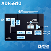
Analog Devices' ADF5610 allows the implementation of fractional-N or integer-N phase-locked loop (PLL) frequency synthesizers when used with an external loop filter and an external reference source. The wideband microwave voltage-controlled oscillator (VCO) design permits frequency operation from 7300 MHz to 14600 MHz at a single radio frequency (RF) output. A series of frequency dividers with a differential frequency output allows operation from 57 MHz to 14600 MHz. Analog and digital power supplies for the PLL circuitry range from 3.1 V to 3.5 V and the VCO supplies are between 4.75 V and 5.25 V. The charge pump supply voltage can be extended up to 3.6 V for improved frequency band overlap and extended upper-frequency range.

The ADF5610 has an integrated VCO with a fundamental frequency of 3650 MHz to 7300 MHz. These frequencies are internally doubled and routed to the RFOUT pin. An additional differential output allows the doubled VCO frequency to be divided by 1, 2, 4, 8, 16, 32, 64, or 128, allowing the user to generate RF output frequencies as low as 57 MHz. A simple 3-wire serial port interface (SPI) provides control of all on-chip registers. To conserve power, this divider block can be disabled when not needed through the SPI interface. Likewise, the output power for both the single-ended output and the differential output are programmable via the VCO register settings. The ADF5610 also contains various power-down modes for the VCO circuitry and PLL circuitry.

Features
  • VCO phase noise: -114 dBc/Hz at 100 kHz from 10 GHz
  • 7 mm x 7 mm integrated solution
  • Wide output frequency range: 57 MHz to 14,600 MHz
  • RFOUT: 7300 MHz to 14,600 MHz
  • PDIV/NDIV: 57 MHz to 14,600 MHz
  • Fractional-N synthesizer and integer-N synthesizer modes
  • 24-bit fractional modulus
  • Exact frequency mode for 0 Hz frequency error
  • Typical PFD spurious: less than -105 dBc
  • Integrated RMS jitter: less than 40 fs
  • Maintains frequency lock over -40°C to +85°C (lock and leave)
  • RFOUT power: 5 dBm
  • Programmable divide by 1, 2, 4, 8, 16, 32, 64, or 128 outputs
  • Programmable output power level
  • Normalized inband phase noise floor FOM
    • High current mode: -232 dBc/Hz (integer) and -229 dBc/Hz (fractional)
    • Normal mode: -229 dBc/Hz (integer) and -226 dBc/Hz (fractional)
  • Low phase noise VCO
    • -115 dBc/Hz typical at 100 kHz (7.3 GHz)
    • -114 dBc/Hz typical at 100 kHz (10 GHz)
    • -109 dBc/Hz typical at 100 kHz (14.6 GHz)
  • Programmable low current and power dissipation: less than 700 mW
  • Fast frequency hopping (autocalibration enabled): less than 40 µs
  • 48-terminal, 7 mm x 7 mm LGA package: 49 mm²
  • Typical power dissipation: 815 mW
Applications
  • Military and defense
  • Test equipment
  • Clock generation
  • Wireless infrastructure
  • Satellite and very small aperture terminal (VSAT)
  • Microwave radio

類別

Top