SN74SSQEA32882ZALR

SN74SSQEA32882ZALR
Mfr. #:
SN74SSQEA32882ZALR
描述:
Registers 28B-56B Reg Buffer
生命週期:
製造商新產品
數據表:
SN74SSQEA32882ZALR 數據表
交貨:
DHL FedEx Ups TNT EMS
支付:
T/T Paypal Visa MoneyGram Western Union
ECAD Model:
更多信息:
SN74SSQEA32882ZALR 更多信息 SN74SSQEA32882ZALR Product Details
產品屬性
屬性值
製造商:
德州儀器
產品分類:
寄存器
RoHS:
Y
最低工作溫度:
0 C
最高工作溫度:
+ 85 C
包裝/案例:
nFBGA-176
打包:
捲軸
系列:
SN74SSQEA32882
品牌:
德州儀器
輸入行數:
/
濕氣敏感:
是的
產品類別:
寄存器
出廠包裝數量:
2000
子類別:
邏輯 IC
單位重量:
0.010935 oz
Tags
SN74SSQ, SN74SS, SN74S, SN74, SN7
Service Guarantees

We guarantee 100% customer satisfaction.

Quality Guarantees

We provide 90-360 days warranty.

If the items you received were not in perfect quality, we would be responsible for your refund or replacement, but the items must be returned in their original condition.
Our experienced sales team and tech support team back our services to satisfy all our customers.

we buy and manage excess electronic components, including excess inventory identified for disposal.
Email us if you have excess stock to sell.

Email: [email protected]
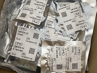
Step1: Vacuum Packaging with PL
Step1:
Vacuum Packaging with PL
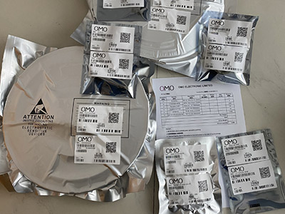
Step2: Anti-Static Bag
Step2:
Anti-Static Bag
Step3: Packaging Boxes
Step3:
Packaging Boxes
    E**o
    E**o
    RU

    All as in the description

    2019-01-09
    A***n
    A***n
    RU

    High quality of product, it matches the description, delivery is fast.

    2019-07-01
    E**i
    E**i
    RU

    All received very quickly. Satisfied with the sender.

    2019-07-13
***ow.cn
Registered Buffer Single-Element 28-CH 176-Pin NFBGA T/R
***as Instruments
810-MHz, JEDEC SSTE32882 compliant 28-bit to 56-bit registered buffer with address-parity test 176-NFBGA 0 to 85
***i-Key
IC REGSTR BUFFER 28-56BIT 176BGA
***i-Key Marketplace
SN74SSQEA32882 JEDEC SSTE32882 C
***INS
This JEDEC SSTE32882-compliant, 28-bit 1:2 or 26-bit 1:2 and 4-bit 1:1 registering clock driver with parity is designed for operation on DDR3 registered DIMMs with VDD of 1.5 V and on DDR3L registered DIMMs with VDD of 1.35 V.
***
All inputs are 1.5 V and 1.35 V CMOS compatible. All outputs are CMOS drivers optimized to drive DRAM signals on terminated traces in DDR3 RDIMM applications. The clock outputs Yn and Yn and control net outputs DxCKEn, DxCSn and DxODTn can be driven with a different strength and skew to optimize signal integrity, compensate for different loading and equalize signal travel speed.
***ASIN
The SN74SSQEA32882 has two basic modes of operation associated with the Quad Chip Select Enable (QCSEN) input. When the QCSEN input pin is open (or pulled high), the component has two chip select inputs, DCS0 and DCS1, and two copies of each chip select output, QACS0, QACS1, QBCS0 and QBCS1. This is the "QuadCS disabled" mode. When the QCSEN input pin is pulled low, the component has four chip select inputs DCS[3:0], and four chip select outputs, QCS[3:0]. This is the "QuadCS enabled" mode. Through the remainder of this specification, DCS[n:0] will indicate all of the chip select inputs, where n=1 for QuadCS disabled, and n=3 for QuadCS enabled. QxCS[n:0] will indicate all of the chip select outputs.
***AS INSTR
The device also supports a mode where a single device can be mounted on the back side of a DIMM. If MIRROR=HIGH, Input Bus Termination (IBT) has to stay enabled for all input signals in this case.
***OMO Electronic
The SN74SSQEA32882 operates from a differential clock (CK and CK). Data are registered at the crossing of CK going HIGH, and CK going LOW. This data could be either re-driven to the outputs or it could be used to access device internal control registers.
***AS INST
The input bus data integrity is protected by a parity function. All address and command input signals are added up and the last bit of the sum is compared to the parity signal delivered by the system at the input PAR_IN one clock cycle later. If they do not match the device pulls the open drain output ERROUT LOW. The control signals (DCKE0, DCKE1, DODT0, DODT1, DCS[n:0]) are not part of this computation.
***AS INSTRUMENTS INCORPORATED
The SN74SSQEA32882 implements different power saving mechanisms to reduce thermal power dissipation and to support system power down states. By disabling unused outputs the power consumption is further reduced.
***ASIN
The package is optimized to support high density DIMMs. By aligning input and output positions towards DIMM finger signal ordering and SDRAM ballout the device de-scrambles the DIMM traces allowing low cross talk design with low interconnect latency.
***as Instr.
Edge controlled outputs reduce ringing and improve signal eye opening at the SDRAM inputs.
Logic Solutions
OMO Electronic Logic Solutions offers a full spectrum of logic functions and technologies from the mature to the advanced, including bipolar, BiCMOS, and CMOS. TI's process technologies offer the logic performance and features required for modern logic designs, while maintaining support for more traditional logic products.Learn More
型號 描述 庫存 價格
SN74SSQEA32882ZALR
DISTI # V72:2272_07360491
Registered Buffer Single 28-CH 176-Pin NFBGA T/R
RoHS: Compliant
2000
  • 1000:$4.0050
  • 500:$5.0330
  • 250:$5.6530
  • 100:$5.8530
  • 25:$6.5960
  • 10:$7.0960
  • 1:$7.8050
SN74SSQEA32882ZALR
DISTI # 296-24877-1-ND
IC REGSTR BUFFER 28-56BIT 176BGA
RoHS: Compliant
Min Qty: 1
Container: Cut Tape (CT)
2365In Stock
  • 1000:$4.7722
  • 500:$5.4792
  • 100:$6.2922
  • 10:$7.6000
  • 1:$8.4100
SN74SSQEA32882ZALR
DISTI # 296-24877-6-ND
IC REGSTR BUFFER 28-56BIT 176BGA
RoHS: Compliant
Min Qty: 1
Container: Digi-Reel®
2365In Stock
  • 1000:$4.7722
  • 500:$5.4792
  • 100:$6.2922
  • 10:$7.6000
  • 1:$8.4100
SN74SSQEA32882ZALR
DISTI # 296-24877-2-ND
IC REGSTR BUFFER 28-56BIT 176BGA
RoHS: Compliant
Min Qty: 2000
Container: Tape & Reel (TR)
Temporarily Out of Stock
  • 2000:$4.4616
SN74SSQEA32882ZALR
DISTI # 26560558
Registered Buffer Single 28-CH 176-Pin NFBGA T/R
RoHS: Compliant
2000
  • 1000:$4.0050
  • 500:$5.0330
  • 250:$5.6530
  • 100:$5.8530
  • 25:$6.5960
  • 10:$7.0960
  • 2:$7.8050
SN74SSQEA32882ZALR
DISTI # SN74SSQEA32882ZALR
Registered Buffer Single 28-CH 176-Pin BGA T/R - Tape and Reel (Alt: SN74SSQEA32882ZALR)
RoHS: Compliant
Min Qty: 2000
Container: Reel
Americas - 12000
  • 2000:$4.2900
  • 4000:$4.2900
  • 8000:$4.2900
  • 12000:$4.2900
  • 20000:$4.2900
SN74SSQEA32882ZALRJEDEC SSTE32882 Compliant 28-Bit to 56-Bit Registered Buffer with Address-Parity Test6000
  • 1000:$3.9000
  • 750:$3.9800
  • 500:$4.6000
  • 250:$5.2900
  • 100:$5.6600
  • 25:$6.3200
  • 10:$6.7600
  • 1:$7.5200
SN74SSQEA32882ZALR
DISTI # 595-74SSQEA32882ZALR
Registers 28B-56B Reg Buffer
RoHS: Compliant
2000
  • 1:$8.1700
  • 10:$7.3800
  • 25:$6.8300
  • 100:$6.1100
  • 250:$5.8000
  • 500:$5.3200
  • 1000:$4.6400
  • 2000:$4.4700
SN74SSQEA32882ZALRPLL Based Clock Driver, SSQE Series, 4 True Output(s), 0 Inverted Output(s), CMOS, PBGA176
RoHS: Compliant
278792
  • 1000:$4.5100
  • 500:$4.7500
  • 100:$4.9500
  • 25:$5.1600
  • 1:$5.5600
SN74SSQEA32882ZALR
DISTI # C1S746202061651
Registered Buffer Single 28-CH 176-Pin NFBGA T/R
RoHS: Compliant
2000
  • 250:$5.6530
  • 100:$5.8530
  • 25:$6.5960
  • 10:$7.0960
  • 1:$7.8050
圖片 型號 描述
SN74SSQEB32882ZALR

Mfr.#: SN74SSQEB32882ZALR

OMO.#: OMO-SN74SSQEB32882ZALR

Registers 28-56 Bit Registered Buffer
SN74SSQEB32882ZALR

Mfr.#: SN74SSQEB32882ZALR

OMO.#: OMO-SN74SSQEB32882ZALR-TEXAS-INSTRUMENTS

Registers 28-56 Bit Registered Buffe
可用性
庫存:
Available
訂購:
1500
輸入數量:
SN74SSQEA32882ZALR的當前價格僅供參考,如果您想獲得最優惠的價格,請提交查詢或直接發送電子郵件至我們的銷售團隊[email protected]
參考價格(美元)
數量
單價
小計金額
1
US$8.17
US$8.17
10
US$7.38
US$73.80
25
US$6.83
US$170.75
100
US$6.11
US$611.00
250
US$5.80
US$1 450.00
500
US$5.32
US$2 660.00
1000
US$4.64
US$4 640.00
由於2021年半導體供不應求,低於2021年之前的正常價格,請發詢價確認。
從...開始
最新產品
  • CC2540 Bluetooth System-on-Chip
    OMO Electronic' CC2540 is a cost-effective, low-power, true system-on-chip (SoC) for Bluetooth® low energy applications.
  • LP5907 Linear Regulator
    LP5907 linear regulators have low quiescent current and lead its class in noise performance without the use for a noise bypass capacitor.
  • CC2630/40/50 SimpleLink Wireless MCUs
    The OMO Electronic' CC2630 / CC2640 / CC2650 family of cost-effective, ultra-low power, 2.4 GHz RF devices have very-low active RF and MCU current.
  • Compare SN74SSQEA32882ZALR
    SN74SSQE32882ZALR vs SN74SSQE32882ZALRBGA vs SN74SSQEA32882ZALR
  • MSP-TS430RGZ48C Target Board
    MSP-TS430RGZ48C target boards feature unified FRAM memory, enhanced MSP430 DNA, and integrated analog and digital peripherals.
  • TPA3144D2 Class-D Audio Power Amplifier
    OMO Electronic' TPA3144D2 is an efficient, Class-D audio power amplifier for driving bridged-tied stereo speakers at up to 6 W, 6 Ω, or 8 Ω (per channel).
Top