CD4055BE

CD4055BE
Mfr. #:
CD4055BE
描述:
LCD Drivers BCD to 7 Segment
生命週期:
製造商新產品
數據表:
CD4055BE 數據表
交貨:
DHL FedEx Ups TNT EMS
支付:
T/T Paypal Visa MoneyGram Western Union
ECAD Model:
更多信息:
CD4055BE 更多信息 CD4055BE Product Details
產品屬性
屬性值
製造商:
德州儀器
產品分類:
液晶驅動器
RoHS:
Y
系列:
CD4055B
位數:
1 Digit
段數:
4:7 Segment
最大時鐘頻率:
8 MHz
工作電源電壓:
3 V to 18 V
電源電流 - 最大值:
300 uA
Pd - 功耗:
500 mW (1/2 W)
最低工作溫度:
- 55 C
最高工作溫度:
+ 125 C
安裝方式:
通孔
包裝/案例:
PDIP-16
打包:
管子
高度:
4.57 mm
長度:
19.3 mm
工作溫度範圍:
- 55 C to + 125 C
產品:
CMOS LCD 驅動器
寬度:
6.35 mm
品牌:
德州儀器
產品類別:
液晶驅動器
出廠包裝數量:
25
子類別:
驅動IC
單位重量:
0.033570 oz
Tags
CD4055BE, CD4055, CD405, CD40, CD4
Service Guarantees

We guarantee 100% customer satisfaction.

Quality Guarantees

We provide 90-360 days warranty.

If the items you received were not in perfect quality, we would be responsible for your refund or replacement, but the items must be returned in their original condition.
Our experienced sales team and tech support team back our services to satisfy all our customers.

we buy and manage excess electronic components, including excess inventory identified for disposal.
Email us if you have excess stock to sell.

Email: [email protected]
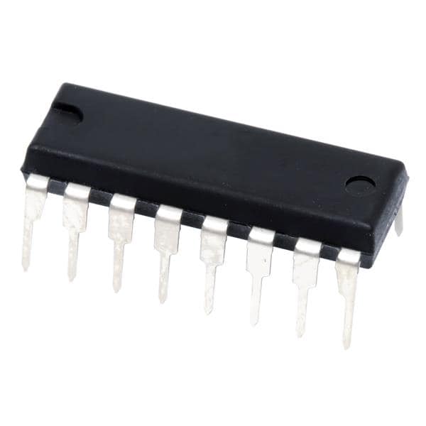
Step1: Vacuum Packaging with PL
Step1:
Vacuum Packaging with PL
Step2: Anti-Static Bag
Step2:
Anti-Static Bag
Step3: Packaging Boxes
Step3:
Packaging Boxes
***as Instruments
CMOS BCD-to-7-Segment LCD Decoder/Driver with Display-Frequency Output 16-PDIP -55 to 125
***ical
Decoder/Driver Single 4-to-7 16-Pin PDIP Tube
***ark
LOGIC, DECODER/DRVR BCD-7, 16DIP
***i-Key
IC DRVR 7 SEGMENT 1 DIGIT 16DIP
***AS INSTUMENTS
CD4055B and CD4056B types are single-digit BCD-to-7-segment decoder/driver circuits that provide level-shifting functions on the chip. This feature permits the BCD input-signal swings (VDD to VSS) to be the same as or different from the 7-segment output-signal swings (VDD to VEE). For example, the BCD input-signal (VDD to VSS) may be as small as 0 to -3 V, whereas the output-display drive-signal swing (VDD to VEE) may be as large as from 0 to -15 V. If VDD to VEE exceeds 15 V, VDD to VSS should be at least 4V (0 to -4V). The 7-segment outputs are controlled by the DISPLAY-FREQUENCY (DF) input which causes the selected segment outputs to be low, high, or a square-wave output (for liquid-crystal displays). When the DF input is low the output segments will be high when selected by the BCD inputs. When the DF input is high, the output segments will be low when selected by the BCD inputs. When a square-wave is present at the DF input, the selected segments will have a square-wave output that is 180° out of phase with the DF input. Those segments which are not selected will have a square-wave output that is in phase with the input. DF square-wave repetition rates for liquid-crystal displays usually range form 30 Hz (well above flicker rate) to 200 Hz (well below the upper limit of the liquid-crystal frequency response). The CD4055B provides a level-shifted high-amplitude DF output which is required for driving the common electrode in liquid-crystal displays. The CD4056B provides a strobed-latch function at the BCD inputs. Decoding of all input combinations on the CD4055B and CD4056B provides displays of 0 to 9 as well as L, P, H, A, -, and a blank position.
***OMO Electronic
The CD4054B provides level shifting similar to the CD4055B and CD4056B independently strobed latches, and common DF control on 4 signal lines. The CD4054B is intended to provide drive-signal compatibility with the CD4055B and CD4056B 7-segment decoder types for the decimal point, colon, polarity, and similar display lines. A level-shifted high-amplitude DF output can be obtained from any CD4054B output line by connecting the corresponding input and strobe lines to a low and high level, respectively and applying a square wave to DFIN. The CD4054B may also be utilized for logic-level "up conversion" or "down conversion". For example, input-signal swings (VDD to VSS) for +5 to 0 V can be converted to output-signal swings (VDD to VEE) of +5 to -5 V. The level-shifted function on all three types permits the use of different input- and output-signal swings. The input swings from a low level of VSS to a high level of VDD while the output swings from a low level of VEE to the same high level of VDD. Thus, the input and output swings can be selected independently of each other over a 3-to 18 V range. VSS may be connected to VEE when no level-shift function is required.
***OMO Electronic
For the CD4054B and CD4056B, data are transferred from input to output by placing a high voltage level at the strobe input. A low voltage at the strobe input latches the data input and the corresponding output segments remain selected (or non-selected) while the strobe is low.
***NS
Whenever the level-shifing function is required, the CD4055B can be used by itself to drive a liquid-crystal display (Fig.16 and Fig.20). The CD4056B, however, must be used together with a CD4054B to provide the common DF output (Fig.19). The capability of extending the voltage swing on the negative end (this voltage cannot be extended on the positive end) can be used to advantage in the setup of Fig.18. Fig.17 is common to all three types.
***AS INSTRUMENT
The CD4054B-, CD4055B-, and CD4056B-series types are supplied in 16-lead dual-in-line plastic packages (E suffix), 16-lead small-outline packages (M, M96, MT and NSR suffixes), and 16-lead thin shrink small-outline packages (PW and PWR suffixes). The CD4054B- and CD4056B-series types also are supplied in 16-lead hermetic dual-in-line ceramic packages (F3A suffix).
圖片 型號 描述
CD4020BE

Mfr.#: CD4020BE

OMO.#: OMO-CD4020BE

Counter ICs 14-Bit Ripple-Carry
CD4026BE

Mfr.#: CD4026BE

OMO.#: OMO-CD4026BE

Counter ICs Decade/Divider
SN7406N

Mfr.#: SN7406N

OMO.#: OMO-SN7406N

Buffers & Line Drivers Hex Inv w/HV Output
BSS138

Mfr.#: BSS138

OMO.#: OMO-BSS138

MOSFET SOT-23 N-CH LOGIC
SN74HC08AN

Mfr.#: SN74HC08AN

OMO.#: OMO-SN74HC08AN

Logic Gates Quad 2-Input Positive-AND Gates
MIC5205-5.0YM5-TR

Mfr.#: MIC5205-5.0YM5-TR

OMO.#: OMO-MIC5205-5-0YM5-TR

LDO Voltage Regulators 150mA 1% Low Noise LDO
MIC5205-5.0YM5-TR

Mfr.#: MIC5205-5.0YM5-TR

OMO.#: OMO-MIC5205-5-0YM5-TR-MICROCHIP-TECHNOLOGY

IC REG LINEAR 5V 150MA SOT23-5
SN7406N

Mfr.#: SN7406N

OMO.#: OMO-SN7406N-TEXAS-INSTRUMENTS

Buffers & Line Drivers Hex Inv w/HV Output
EPS-65S-24

Mfr.#: EPS-65S-24

OMO.#: OMO-EPS-65S-24-MEAN-WELL

AC/DC Power Supply Single-OUT 24V 2.98A 65W 6-Pin
SN74HC08AN

Mfr.#: SN74HC08AN

OMO.#: OMO-SN74HC08AN-1190

QUAD 2-INPUT POSITIVE-AND GATES
可用性
庫存:
Available
訂購:
1984
輸入數量:
CD4055BE的當前價格僅供參考,如果您想獲得最優惠的價格,請提交查詢或直接發送電子郵件至我們的銷售團隊[email protected]
參考價格(美元)
數量
單價
小計金額
1
US$0.55
US$0.55
10
US$0.45
US$4.52
100
US$0.28
US$27.50
1000
US$0.21
US$213.00
2500
US$0.18
US$455.00
10000
US$0.17
US$1 690.00
25000
US$0.16
US$4 000.00
50000
US$0.16
US$7 850.00
從...開始
最新產品
  • bq25700A Battery Buck-Boost Charge Controller
    OMO Electronic offers the bq25700A SMBus multi-chemistry battery buck-boost charge controller with system power monitor and processor hot monitor.
  • TMUX1208 Analog Multiplexer (Mux)
    OMO Electronic' TMUX1208 general purpose analog mux reduces system complexity and board size in a wide variety of applications including building automation.
  • TPD3S014/44 Current Limit Switch
    OMO Electronic' TPD3S014/44’s are integrated devices that feature a current limited load switch and a two channel Transient Voltage Suppressor (TVS).
  • Compare CD4055BE
    CD4055BE vs CD4055BEE4 vs CD4055BEG4
  • OPA388 Operational Amplifier
    OMO Electronic' OPA388 precision op-amp provides rail-to-rail input output operation in a low-noise, zero-drift, zero-crossover device.
  • TLV9052 RRIO Op-Amp
    OMO Electronic' TLV9052 5 MHz, low-power, RRIO op-amp offers an ultra-high slew rate and low supply current per channel providing excellent AC performance.
Top