SN74ABT7819A-10PH

SN74ABT7819A-10PH
Mfr. #:
SN74ABT7819A-10PH
描述:
FIFO 512x18x2 Clocked Bidir Mem
生命週期:
製造商新產品
數據表:
SN74ABT7819A-10PH 數據表
交貨:
DHL FedEx Ups TNT EMS
支付:
T/T Paypal Visa MoneyGram Western Union
ECAD Model:
更多信息:
SN74ABT7819A-10PH 更多信息 SN74ABT7819A-10PH Product Details
產品屬性
屬性值
製造商:
德州儀器
產品分類:
先進先出
RoHS:
N
包裝/案例:
QFP-80
品牌:
德州儀器
安裝方式:
貼片/貼片
產品類別:
先進先出
出廠包裝數量:
1
子類別:
內存和數據存儲
單位重量:
0.061338 oz
Tags
SN74ABT7819A-1, SN74ABT7819A, SN74ABT781, SN74ABT7, SN74AB, SN74A, SN74, SN7
Service Guarantees

We guarantee 100% customer satisfaction.

Quality Guarantees

We provide 90-360 days warranty.

If the items you received were not in perfect quality, we would be responsible for your refund or replacement, but the items must be returned in their original condition.
Our experienced sales team and tech support team back our services to satisfy all our customers.

we buy and manage excess electronic components, including excess inventory identified for disposal.
Email us if you have excess stock to sell.

Email: [email protected]
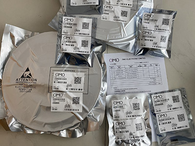
Step1: Vacuum Packaging with PL
Step1:
Vacuum Packaging with PL
Step2: Anti-Static Bag
Step2:
Anti-Static Bag
Step3: Packaging Boxes
Step3:
Packaging Boxes
***i-Key
IC SYNC FIFO MEM 512X18X2 80-QFP
***as Instruments
A FIFO memory is a storage device that allows data to be written into and read from its array at independent data rates. The SN74ABT7819A is a high-speed, low-power, BiCMOS, bidirectional, clocked FIFO memory. Two independent 512 18 dual-port SRAM FIFOs (FIFOA, FIFOB) on the chip buffer data in opposite directions. Each FIFO has flags to indicate empty and full conditions, a half-full flag, and a programmable almost-full/almost-empty flag. The SN74ABT7819A is a clocked FIFO, which means each port employs a synchronous interface. All data transfers through a port are gated to the low-to-high transition of a continuous (free-running) port clock by enable signals. The continuous clocks for each port are independent of one another and can be asynchronous or coincident. The enables for each port are arranged to provide a simple bidirectional interface between microprocessors and/or buses with synchronous control. The state of the A0–A17 outputs is controlled by the port-A chip select (CSA)\ and the port-A write/read select (W/R\A). When both CSA\ and W/R\A are low, the outputs are active. The A0–A17 outputs are in the high-impedance state when either CSA\ or W/R\A is high. Data is written to FIFOA–B from port A on the low-to-high transition of the port-A clock (CLKA) input when CSA\ is low, W/R\A is high, the port-A write enable (WENA) is high, and the port-A input-ready (IRA) flag is high. Data is read from FIFOB–A to the A0–A17 outputs on the low-to-high transition of CLKA when CSA\ is low, W/R\A is low, the port-A read enable (RENA) is high, and the port-A output-ready (ORA) flag is high. The state of the B0–B17 outputs is controlled by the port-B chip select (CSB)\ and the port-B write/read select (W/R\B). When both CSB\ and W/R\B are low, the outputs are active. The B0–B17 outputs are in the high-impedance state when either CSB\ or W/R\B is high. Data is written to FIFOB–A from port B on the low-to-high transition of the port-B clock (CLKB) when CSB\ is low, W/R\B is high, the port-B write enable (WENB) is high, and the port-B input-ready (IRB) flag is high. Data is read from FIFOA–B to the B0–B17 outputs on the low-to-high transition of CLKB when CSB\ is low, W/R\B is low, the port-B read enable (RENB) is high, and the port-B output-ready (ORB) flag is high. The setup- and hold-time constraints for the chip selects (CSA\, CSB)\ and write/read selects (W/R\A, W/R\B) enable write and read operations on memory and are not related to the high-impedance control of the data outputs. If a port read enable (RENA or RENB) and write enable (WENA or WENB) are set low during a clock cycle, the chip select and write/read select can switch at any time during the cycle to change the state of the data outputs. The input-ready (IR) and output-ready (OR) flags of a FIFO are two-stage synchronized to the port clocks for use as reliable control signals. CLKA synchronizes the status of the input-ready flag of FIFOA–B (IRA) and the output-ready flag of FIFOB–A (ORA). CLKB synchronizes the status of the input-ready flag of FIFOB–A (IRB) and the output-ready flag of FIFOA–B (ORB). When the IR flag of a port is low, the FIFO receiving input from the port is full and writes are disabled to its array. When the OR flag of a port is low, the FIFO that outputs data to the port is empty and reads from its memory are disabled. The first word loaded to an empty memory is sent to the FIFO output register at the same time its OR flag is asserted (high). When the memory is read empty and the OR flag is forced low, the last valid data remains on the FIFO outputs until the OR flag is asserted (high) again. In this way, a high on the OR flag indicates new data is present on the FIFO outputs. The SN74ABT7819A is characterized for operation from 0C to 70C.
圖片 型號 描述
SN74ABT7819A-30PH

Mfr.#: SN74ABT7819A-30PH

OMO.#: OMO-SN74ABT7819A-30PH

FIFO 512x18x2 Clocked Bidir Mem
SN74ABT7820-20PN

Mfr.#: SN74ABT7820-20PN

OMO.#: OMO-SN74ABT7820-20PN

FIFO 512 x 18 x 2 bidir ASynch FIFO Memory
SN74ABT7819-12PH

Mfr.#: SN74ABT7819-12PH

OMO.#: OMO-SN74ABT7819-12PH-1190

Bi-Directional FIFO, 512X18, 9ns, Synchronous, BICMOS, PQFP80
SN74ABT7819-20PN

Mfr.#: SN74ABT7819-20PN

OMO.#: OMO-SN74ABT7819-20PN-1190

Bi-Directional FIFO, 512X18, 12ns, Synchronous, BICMOS, PQFP80
SN74ABT7819A-10PN

Mfr.#: SN74ABT7819A-10PN

OMO.#: OMO-SN74ABT7819A-10PN-TEXAS-INSTRUMENTS

IC SYNC FIFO MEM 512X18X2 80LQFP
SN74ABT7820-30PH

Mfr.#: SN74ABT7820-30PH

OMO.#: OMO-SN74ABT7820-30PH-TEXAS-INSTRUMENTS

FIFO 512 x 18 x 2 bidir ASynch FIFO Memory
SN74ABT7820-15PH

Mfr.#: SN74ABT7820-15PH

OMO.#: OMO-SN74ABT7820-15PH-TEXAS-INSTRUMENTS

FIFO 512 x 18 x 2 bidir ASynch FIFO Memory
SN74ABT7820-25PH

Mfr.#: SN74ABT7820-25PH

OMO.#: OMO-SN74ABT7820-25PH-TEXAS-INSTRUMENTS

FIFO 512 x 18 x 2 bidir ASynch FIFO Memory
SN74ABT7820-15PN

Mfr.#: SN74ABT7820-15PN

OMO.#: OMO-SN74ABT7820-15PN-TEXAS-INSTRUMENTS

FIFO 512 x 18 x 2 bidir ASynch FIFO Memory
SN74ABT7819A-12PN

Mfr.#: SN74ABT7819A-12PN

OMO.#: OMO-SN74ABT7819A-12PN-TEXAS-INSTRUMENTS

FIFO 512x18x2 Clocked Bidir Mem
可用性
庫存:
Available
訂購:
2500
輸入數量:
SN74ABT7819A-10PH的當前價格僅供參考,如果您想獲得最優惠的價格,請提交查詢或直接發送電子郵件至我們的銷售團隊[email protected]
從...開始
最新產品
Top