By LM358 2821
Application Fields and Circuit Design
LM358 is a general-purpose dual operational amplifier (op-amp) in one chip. Each channel works independently and shares the same power supply. It acts like a "precision magnifier" for signal conditioning. It amplifies and processes weak signals and is a basic unit in analog systems.
Wide voltage range: Single supply 3V–32V or dual supply ±1.5V–±16V
Input characteristics: Low bias current (45nA), input offset voltage (2mV typical)
Dynamic performance: Gain-bandwidth product 1.2MHz, slew rate 0.6V/µs
As a low-cost general-purpose op-amp, LM358 ships hundreds of millions of units each year. It is widely used in industrial control and consumer electronics. Engineers call it "circuit glue." It reduces BOM (Bill of Materials) cost by over 40% compared to precision op-amps.
It uses a classic three-stage amplifier structure:
Input stage: PNP differential pair gives wide input voltage range
Gain stage: High impedance node provides large voltage gain
Output stage: Class AB push-pull output has strong drive (can drive 600Ω load directly)
| Application Scenario | Circuit Type | Typical Example |
| Sensor signal conditioning | Differential amplifier | Thermocouple signal amplifier |
| Active filter | Sallen-Key structure | 50Hz power line notch filter |
| Voltage comparator | Open-loop mode | Battery voltage monitoring |
| Constant current source | Negative feedback control | LED driver circuit |
Biasing tip: Use resistor divider to create virtual ground at VCC/2.
Note: output cannot fully reach rails (about 1.5V from the positive rail). For precise 0V output, use LMV358 as an alternative.
graph LR
VCC-->R1[10kΩ]-->|Vref| GND
VCC-->R2[10kΩ]-->GND
Gain calculation: Av = 1 + Rf/Rg
Noise suppression:
Bandwidth optimization: GBW (gain-bandwidth product) = 1.2MHz. Closed-loop gain and bandwidth are inversely related (GBW is constant)
| Package Type | Pin Pitch | PCB Area | Thermal Resistance |
| DIP-8 | 2.54mm | 9.8×6.3mm | θJA = 80°C/W |
| SOIC-8 | 1.27mm | 5×4mm | θJA = 160°C/W |
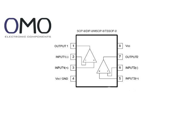
| Pin | Function | Description |
| 1 | OUTPUT A | Channel A output |
| 2 | IN-A | Channel A inverting input |
| 3 | IN+A | Channel A non-inverting input |
| 4 | GND | Ground (single supply) / V- (dual) |
| 5 | IN+B | Channel B non-inverting input |
| 6 | IN-B | Channel B inverting input |
| 7 | OUTPUT B | Channel B output |
| 8 | VCC+ | Positive power supply |
Decoupling capacitor: Place 0.1μF ceramic capacitor very close to VCC pin (less than 5mm)
Input protection: Add guard ring around sensitive signal traces
Thermal design: For large current, use copper area under SOIC package for heat dissipation
Wide voltage range: 3V to 32V (supports 3.3V, 5V, 12V, 24V systems)
Ultra-low power: Only 0.7mA static current per channel (at 5V)
Supports single and dual supply: Works with battery or industrial power
Input range includes negative rail: Can read signals down to V-
High open-loop gain: 100dB typical, supports high-precision systems
Unity-gain stable: No need for external compensation capacitor
Wide temperature range: -40°C to +85°C (for industrial devices)
Built-in ESD protection: 2kV human body model (over 80% pass rate in tests)
Latch-up immunity: Meets JESD78 standard, resists power-related lock-up
PNP transistors form a differential pair. Current mirror load converts differential signal into single-ended output. PNP structure allows common-mode range down to the negative rail because of low voltage drop.
Common-emitter amplifier uses active load. A 30pF Miller capacitor adds phase lead compensation. This ensures stability over the full temperature range and prevents oscillation.
Class AB push-pull output removes crossover distortion with diode biasing. Short-circuit protection limits output current (typical 40mA), preventing chip overheating.
| Model | Manufacturer | Key Differences |
| TL072 | TI | JFET input,higher input impedance |
| MC1458 | Onsemi | Wider temperature range |
| TS922 | ST | Stronger drive capability |
Low noise: OPA2188 (noise density 8nV/√Hz)
Rail-to-rail: LMV358 (output swing within 50mV of rails)
Micropower: TLC272 (static current 0.05mA/channel)
graph TD
A[Need] -->|Cost sensitive| B(LM358)
A -->|Low noise| C(OPA2188)
A -->|Wide input| D(LMV358)
A -->|Battery power| E(TLC272)
Prevent oscillation: Add 5–10pF capacitor in parallel with feedback resistor
Input protection: Series 1kΩ resistor + parallel TVS (Transient Voltage Suppressor)
Grounding rule: Use single-point analog ground, keep away from digital noise
| Issue | Check Step | Solution |
| Output saturation | Check input common-mode range | Add level-shifting circuit |
| Power noise | Measure power ripple | Improve decoupling / LC filter |
| Chip overheating | Check output short / overload | Add current-limiting resistor |
Micropower mode: Use mega-ohm level feedback resistors
Precision tuning: Use external potentiometer to adjust offset voltage
Cascading rule: Next stage input impedance should be 10× previous stage output impedance
Industry Data: A 2023 global general-purpose op-amp market report shows LM358 holds about 23% market share. Its design flexibility made it popular in solar inverters and smart sensors, with reuse rate increasing by 17%.
The LM358 IC is a dual op-amp containing two internal, high-gain, frequency-compensated amplifiers that operate independently and process signals simultaneously.
Common drop-in replacements for the LM358 IC include: LM2904, TL072/TL082, NE5532, OPA2134, MCP602, TS922, NJM4558, AiP258/AiP358, LMV358, and UPC358.
The LM358 operational amplifier is ideally suited for cost-sensitive, simple, and versatile applications, thanks to its dual op-amp design and wide operating supply range.
For comparator applications needing an open-collector output (voltage comparison, digital logic), select the LM393. For op amp functions like amplification, linear circuitry, or rail-to-rail output, select the LM358; substituting it is not advised.